915 MHz MPCVD reactors for large-area diamond growth
Carat Systems develops high-power 915 MHz microwave plasma CVD reactor platforms for large-area diamond growth, seed production, and scale-up beyond the practical plasma footprint of conventional 2.45 GHz systems.
Large-area diamond growth is a coupled reactor, process, and materials problem. Carat works with customers to define the plasma footprint, power and pressure envelope, substrate coupling, thermal gradients, edge behavior, film stress, uniformity targets, metrology plan, and path from prototype development to production.
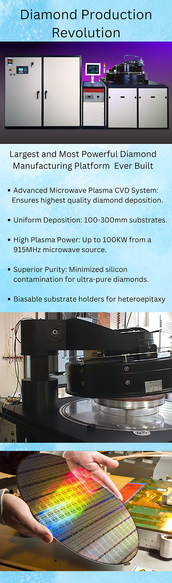
915 MHz high-power microwave plasma CVD platform for large-area diamond coating and scale-up development.
Why use a 915 MHz MPCVD reactor for large-area diamond growth?
Scaling CVD diamond from 100 mm toward 150 mm, 200 mm, and 300 mm class substrates limiting factors are plasma footprint, field structure, substrate coupling, heat removal, edge effects, and film stress.
A 915 MHz high-power MPCVD reactor provides a path to a larger plasma volume and higher total microwave power. This supports development programs where 2.45 GHz systems become constrained by plasma diameter, total power, thermal uniformity, or the available operating window.
Large-area diamond scale-up should be treated as a reactor-process-materials problem, not only a higher-power version of small-area growth. The relevant design variables include plasma footprint, substrate overfill, pressure, gas residence time, stage coupling, edge compensation, wall and gas losses, thermal gradients, metrology access, and the target quality metric.
Large plasma footprint
Supports development toward 150 mm to 300 mm class coating areas.
High total power
Enables process windows that are difficult to access with smaller 2.45 GHz platforms.
Scale-up engineering
Focuses on coupling, thermal management, fixturing, edge compensation, and uniformity instead of chemistry alone.
Configured around the application
Carat's 915 MHz work is offered as an application-specific reactor and process-development program rather than a one-size-fits-all production tool. Final power, pressure range, stage design, diagnostics, chamber geometry, and substrate capacity are defined against the customer's measurable film and throughput requirements.
Target applications
- Large-area polycrystalline CVD diamond wafers
- Diamond-on-silicon thermal spreaders
- Diamond-on-semiconductor process development
- High-power electronics thermal management
- Optical and electronic grade diamond scale-up
- Seed production for single-crystal diamond growth
- Custom large-area coating development
Development approach
- Define substrate size, thickness target, and film quality requirements
- Evaluate thermal coupling, fixture design, and edge control
- Develop uniformity, bow, and Raman quality targets at smaller scale first
- Transition from 2.45 GHz process knowledge into 915 MHz scale-up
- Use sample coating and process development to reduce scale-up risk
- Connect reactor design, process window, metrology, and production path
Prototype design versus production optimization
For large-area CVD diamond, a prototype should be designed with enough power, pressure range, diagnostic access, and thermal flexibility to avoid being hardware-limited during process discovery. The optimized production point can then be selected against measured thickness uniformity, Raman quality, morphology, stress, growth rate, edge exclusion, and operating cost.
This distinction is important. A development platform should expose the useful process window and reveal the dominant technical constraints. A production system can then be simplified, narrowed, and optimized after the process requirements are measured.
De-risking 300 mm class diamond coating
Carat's scale-up work indicates that larger-area diamond growth becomes increasingly sensitive to thermal engineering, edge effects, field structure, plasma overfill, and substrate coupling. The 915 MHz platform is intended for programs where a larger plasma footprint and higher total power are required to support a credible path toward 300 mm class diamond coating.
- 100 mm, 10 kW, 2.45 GHz operation supports stable and reproducible diamond growth.
- 150 mm to 200 mm scale introduces stronger thermal and coupling constraints.
- 915 MHz high-power operation has demonstrated a plasma footprint relevant to 300 mm class development.
- Final system requirements depend on target substrate size, edge exclusion, growth rate, film quality, thermal design, and application-specific metrics.
Start with a 915 MHz design-basis review
Before committing to a full reactor or scale-up program, Carat can review the application and define a technically credible starting point. The review can address substrate constraints, likely deposition regime, power and pressure envelope, thermal risks, diagnostic access, development stages, and the transition from process discovery to equipment or production.
Useful applications
- Diamond-on-semiconductor and large-area thermal spreaders
- 150 mm, 200 mm, and 300 mm class diamond growth
- Optical, electronic, and polycrystalline diamond scale-up
- Fusion-target and custom-substrate coating programs
- High-volume seed production
Information to send
- Substrate material, diameter, thickness, and allowable edge exclusion
- Target diamond thickness, growth rate, and quality metrics
- Uniformity, stress, bow, Raman, or morphology requirements
- Desired production rate or number of substrates per run
- Current process data, equipment limits, or development status
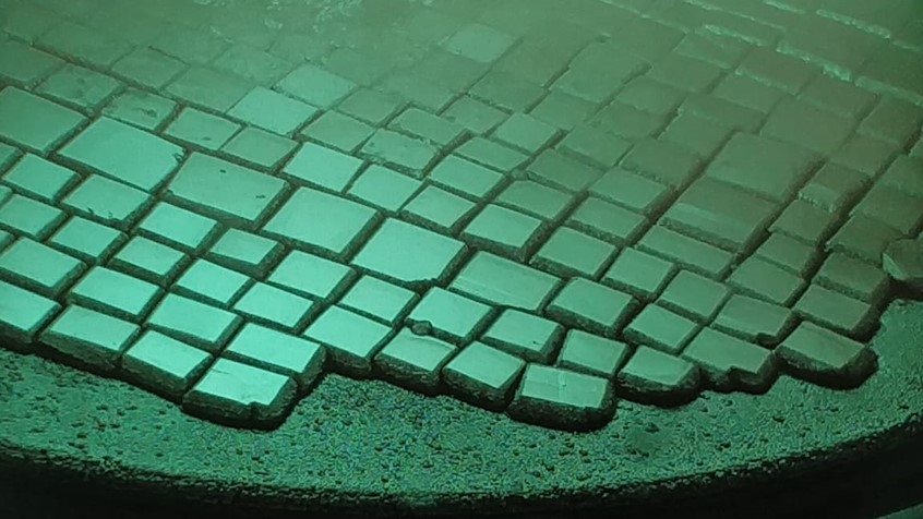
Large plasma area for simultaneous diamond seed production and scale-up development.
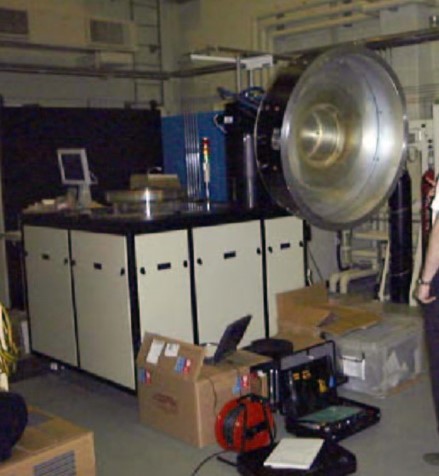
Side-opening chamber design for cleaning, service access, and large-area process development.